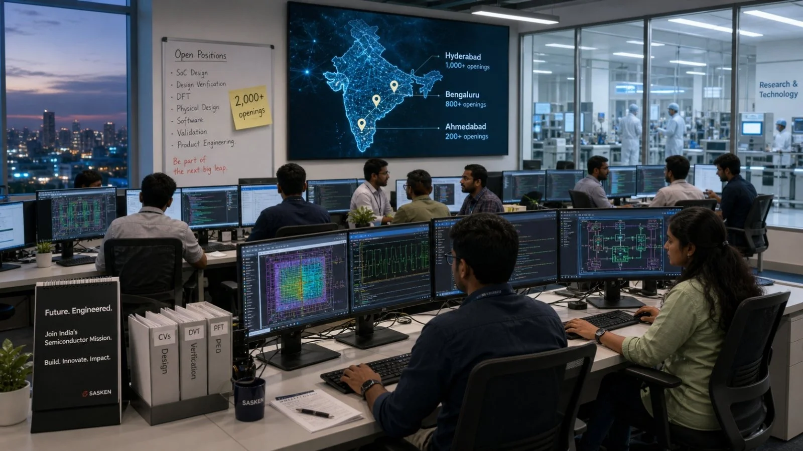
Semiconductor hiring in India is no longer a Bengaluru-only story. Hyderabad and Gujarat are making their mark even as the broader market’s growth rate eases. The country’s GCCs have put over 65,000 people to work, up some 3 percent in the past year. You can see in this spread that India is moving on from being a design back-office to something more like a manufacturing ecosystem.
It’s a matter of strategy. There is a $10-billion effort to make good on India’s design chops and turn them into hard industrial muscle, with an eye on building a supply chain that can deliver.
Xpheno’s numbers show net hiring has levelled off to about 2,000 in the last 12 months, but there is still plenty of action with 2,000-odd open positions. The profile of the hire is changing: it’s not just for engineers anymore, but for those with a hand in operations and the like.
“Right now we have 2,000 active demands, 78 percent of them in engineering,” says Kedar Pathak, a talent specialist at Xpheno. He is seeing a lot of need for systems design, SoC, and verification.
Hyderabad is one of the winners in this shift. It is home to roughly 9,300 in the field and has put up 4 percent growth. Delhi NCR is in the 2,200 range with the same kind of numbers. Then you have Ahmedabad, which is moving fast – 36 percent on top of a 1,000-strong base.
“The India Semiconductor Mission has made us more than a place for design; we are building out the whole value chain,” says Medha Kannapally of Endiya Partners. Pathak puts it another way: you can find semi-skilled help now, but be ready for a bump in demand for lower-skilled jobs. “We’re looking at a 30% jump in unskilled labour this year, for technicians who know silicon processing.” It shows where the new money is going: to the factories and the suppliers, not just the design labs.
Our engineers are the brain trust of the industry, making up close to 20% of the global IC design headcount. You’ll find them in the 125,000 or so who work for Intel, Qualcomm, AMD and the like.
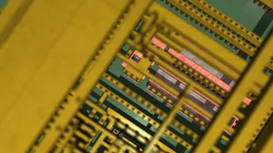
But for a long time, we let the unglamorous side of things – the fabs – lag. We didn’t put in the work on specialty chemicals, power, or the kind of supplier density you need. The 1989 fire at the Mohali lab was a case in point. Now, with home-grown demand set to pass $100 billion by 2030, we have to be in the game.
Policy tailwinds and market positioning
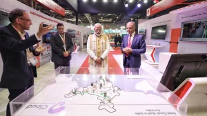
Policy is getting real about it. The ISM has given the green light to ten projects across six states, worth some Rs.1.6 lakh crore. The 2026 Union Budget is putting teeth in it, with moves to link chips to data and materials.
Key policy levers announced or reinforced recently include:
– Rs 40,000-crore Electronics Components Manufacturing Scheme
– Tax incentives for global data centre investments
– Rare-earth processing corridors in development
– Incentives for container manufacturing capacity
– SEZ reforms enabling greater domestic access
You can’t ignore data centres. AI is eating up the most advanced chips, so semiconductor policy is inextricably linked to digital infrastructure. It’s about shortening the path from raw material to compute.
Look at the rest of the world. Hsinchu in Taiwan has its discipline. South Korea has its champions. The US is in a rebuild with the CHIPS Act. China is throwing money at it.
Clusters, not sprawl, will decide winners
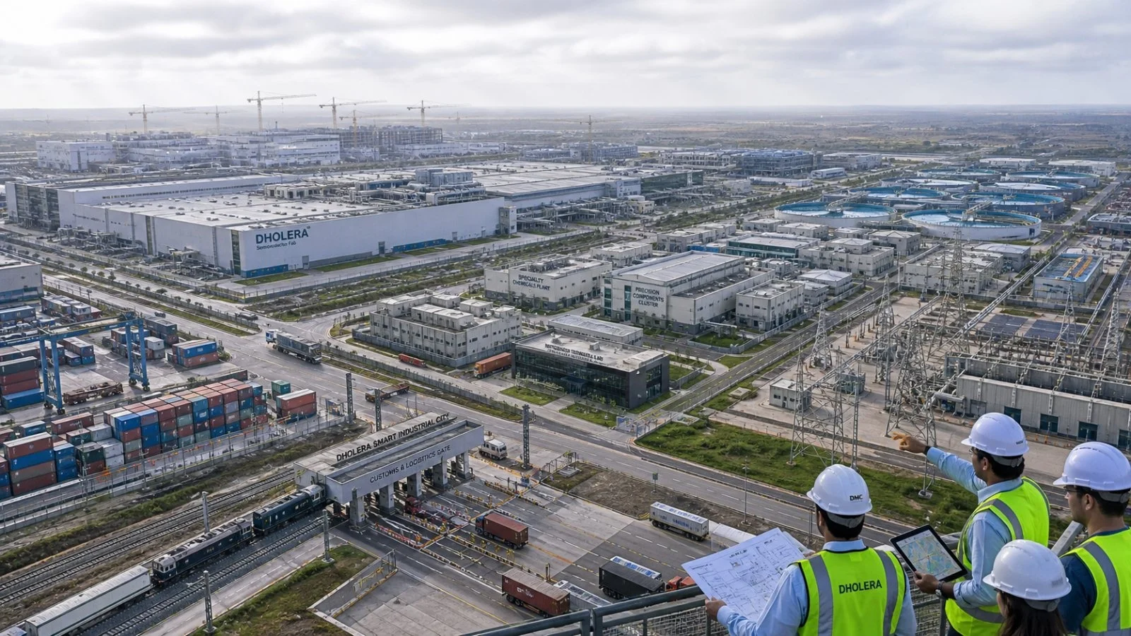
This is an ecosystem business. India needs to get focused. Dholera in Gujarat, with PSMC setting up shop, is a start. We want two or three clusters that can hold their own, not a few sites here and there.
What makes or breaks it is the stuff you don’t see in the news: water purity, a grid you can count on, customs that don’t tie you up, and logistics that are on time. In this line of work, your infrastructure is your strategy.
Phased playbook, not a moonshot
Packaging is the way in for now. Phase 1 (2026-2027) is about scaling ATMP, with Micron in Gujarat as an example. With AI, packaging is a performance issue, not an afterthought.
Down the road, in Phase 3 (2030-2033), we should be in a position to lead on the hard stuff: chiplets, 3D packaging, and heterogeneous integration. That’s where our design and system skills can shine.
In between, Phase 2 (2027-2030) is for the mature and specialty nodes – the kind of semis you need for EVs, the grid, and defence. These are big, doable markets.
After you have all that in place, then you can think about Phase 4 (2033-2036): some selective, high-end fabrication with the right partners.
People and suppliers will make or break it
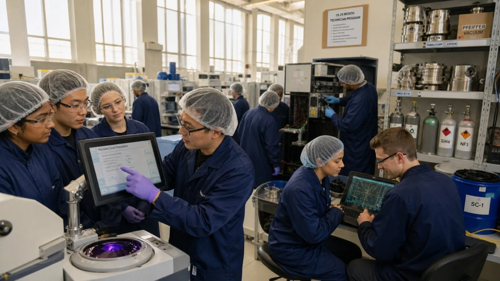
Then there is the human side. We have to train up the fab technicians, the yield experts, the ones who keep the equipment running. Manufacturing is about knowledge you can’t put in a manual. We need 18- to 24-month programmes for that.
And we can’t forget the suppliers in the middle. The chemical and gas companies, the tool makers – they have to be on the ground. Hsinchu and Seoul will tell you: if you don’t have the thousands of suppliers around you, you don’t have resilience.
From participant to indispensable node
We don’t have to be Taiwan or the US. We can be something else: a mix of top-tier design and the kind of scale and integration that is uniquely ours.
It’s not about dethroning Silicon Valley. It’s about being the part of the supply chain for AI and secure electronics that the world can’t do without.
Hiring is in new places, the clusters are forming, and the policy is in step with what we can actually do. For once, this isn’t just talk. It’s within our grasp.